CARBON
NANOTUBES
Discovery
of Carbon Nanotube
Sumio Iijima (born May 2, 1939) is a Japanese physicist,
often cited as the discoverer of carbon
nanotubes. In 1991 he observed Multiwalled carbon Nanotube and in
1993 he discovers Single wall carbon Nanotube. For this and other work Sumio Iijima was
awarded, together with Louis Brus, the inaugural Kavli Prize
for Nanoscience in 2008.
Introduction
Carbon nanotubes (CNTs) also called buckytubes are
allotropes of carbon with a cylindrical
nanostructure.
Basic Structure:
A single layer of graphite is called graphene
and has extraordinary electrical, thermal, and physical properties.
Carbon
nanotube (CNT) is a new form of carbon, configurationally equivalent to two
dimensional graphene sheet rolled into a tube.The ends of a nanotube might be
capped with a hemisphere of the buckyball structure. It is just a few nanometers in diameter and several
microns long.They are light, flexible, thermally stable, and are chemically
inert. They have the ability to be either metallic or semi-conducting depending
on the "twist" of the tube.
Nanotubes are categorized as single-walled
nanotubes (SWNTs) and multi-walled
nanotubes (MWNTs).

Single-walled
Nanotube (SWNTs)

It
is equivalent to two dimensional graphene sheet rolled into a tube. Single-walled Nanotube can
be considered as one-dimensional quantum wire.
Types of SWNTs

Nanotubes
form different types, which can be described by the chiral vector (n, m), where n and m are integers of the vector equation
R = na1 + ma2. The chiral vector is
determined by the diagram below.

Imagine
that the nanotube is unraveled into a planar sheet. Draw two lines along the
tube axis where the separation takes place. In other words, if you cut along
the two lines and then match their ends together in a cylinder, you get the
nanotube that you started with. Now, find any point on one of the lines that
intersects one of the carbon atoms (point A). Next, draw the Armchair line,
which travels across each hexagon, separating them into two equal halves. Now
that you have the armchair line drawn, find a point along the other tube axis
that intersects a carbon atom nearest to the Armchair line (point B). Now
connect A and B with our chiral vector, R.The wrapping angle ф, is formed between R and the Armchair
line. If R lies along the Armchair line (ф=0°),
then it is called an "Armchair" nanotube. If ф =30°, then the tube is of the "zigzag" type.
Otherwise, if 0°< ф <30° then
it is a "chiral" tube. The vector a1 lies along the
"zigzag" line.The other vector a2 has a different
magnitude than a1, but its direction is a reflection of a1
over the Armchair line. When added together, they equal the chiral vector R.
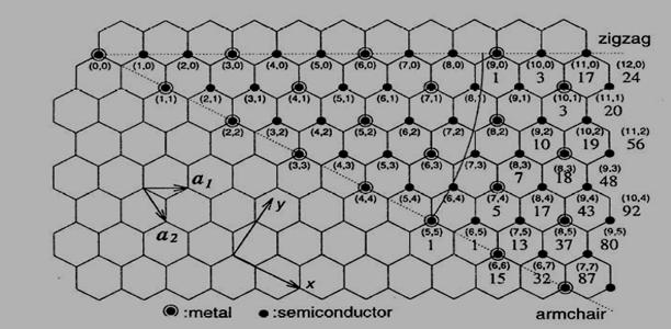
The
values of n and m determine the chirality, or
"twist" of the nanotube. The chirality in turn affects the
conductance of the nanotube, its density, its lattice structure, and other
properties.A SWNT is considered metallic if the value n - m is divisible by three or zero. Otherwise, the nanotube is
semiconducting. Consequently, when tubes are formed with random values of n and m, we would expect that two-thirds of nanotubes would be
semi-conducting, while the other third would be metallic. Another important parameter is
the chiral angle, which is the angle between R and â1.Given
the chiral vector (n, m), the
diameter of a carbon nanotube can be determined using the relationship
d = (n2 + m2 + nm) 1/2 0.0783 nm
Chiral angle = tan-1(Ö3n/(2m + n)).
|
|
|
|
|
|
Ropes of Carbon Nanotubes

In
1996, Thess et al. measured the
properties of "ropes" of carbon nanotubes. As shown
in the diagram at right, ropes are bundles of tubes packed together in an
orderly manner. They found that the individual SWNTs packed into a close-packed
triangular lattice with a lattice constant of about 17 Å. As a good
estimate,the lattice parameter in CNT ropes (bundled nanotubes) is d + 0.34 nm, where d is the tube diameter given above.
Multiwalled Carbon nanotubes
Multi-walled nanotubes (MWNT) consist of multiple
rolled layers (concentric tubes) of
graphite. There are two models which can be used to describe the structures
of multi-walled nanotubes.
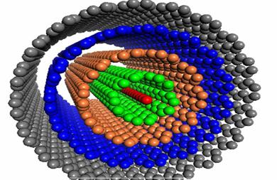
In the Russian Doll
model, sheets of graphite are arranged in concentric cylinders, e.g. a (0, 8)
single-walled nanotube (SWNT) within a larger (0, 10) single-walled nanotube.
In the Parchment model, a single sheet of
graphite is rolled in around itself, resembling a scroll of parchment or a rolled
newspaper. The interlayer distance in multi-walled nanotubes is close to the
distance between graphene layers in graphite, approximately 3.4 Å.
Properties Of CNT:
Physical Properties:
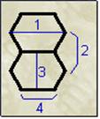
|
Average Diameter of SWNT |
1.2-1.4 nm |
|
Distance from opposite carbon atoms
(Line 1) |
2.83 A |
|
Analogous Carbob atom separation(line
2) |
2.456 A |
|
Parallel carbon bond separation(line
3) |
2.45 A |
|
Carbon bond length(line4) |
1.42 A |
|
C – C tight bonding overlap energy |
~ 2.5 ev |
|
Lattice constant |
17 A |
|
Density (10,10) Armchair (17,0) Zigzag (12,6) Chiral |
1.33 g/cm3 1.34
g/cm3 1.40 g/cm3 |
|
Interlayer Spacing (n,n) Armchair (n,0) Zigzag (2n,n) Chiral |
3.38 Å 3.41Å 3.39 Å |
Optical Properties:
Fundamental Gap:
For (n, m); n-m is divisible by 3 [Metallic] 0 eV
For (n, m); n-m is not divisible by 3 [Semi-Conducting] ~ 0.5 eV
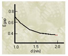
The fundamental gap
(HOMO-LUMO) of semiconductor was a function of diameter ,where gap was in the
order of about of 0.5eV.
Egap=2y0acc/d
Where y0 is the
C-C tight bonding overlap energy (2.7![]() 0.1 eV), acc is the nearest distance (0.142nm),and d
is the diameter.
0.1 eV), acc is the nearest distance (0.142nm),and d
is the diameter.
Density of states:

Calculating the density of states for small
structures shows that the distribution of electrons changes as dimensionality
is reduced. For quantum wires, the DOS for certain energies
actually becomes higher than the DOS for bulk semiconductors, and for quantum dots
the electrons become quantized to certain energies.
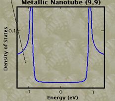
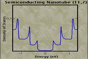
At
the Fermi Energy (the highest occupied energy level), the density of states
finite for a metallic tube (though very small), and zero for a semi-conducting
tube. As energy is increased, sharp peaks in the density of states, called Van
Hove singularities, appear at specific energy levels.
Electrical Properties:
Resistance 6500 Ω
Maximum Current Density 1013
A/m2
Thermal Properties:
Thermal
Conductivity ~2000 W /m-K
Phonon Mean Free Path ~ 100 nm
Relaxation Time ~ 10-11 s
Elastic Properties:
Young's Modulus (SWNT) ~ 1
Tpa
Young's Modulus (MWNT) 1.28 Tpa
Maximum Tensile Strength ~30 Gpa
Electronic
Properties of Nanotubes:
The unique electronic properties of carbon
nanotubes are due to the quantum confinement of
electrons normal to the nanotube axis. In the
radial direction, electrons are confined by the monolayer thickness of the
graphene sheet. Around the circumference of the nanotube, periodic boundary
conditions come into play. For example, if a zigzag or armchair nanotube has 10
hexagons around its circumference, the 11th hexagonal will coincide with the
first. Going around the cylinder once introduces a phase difference of
2∏.Because of this quantum confinement, electrons can only propagate
along the nanotube axis, and so their wavevectors point in this direction.
These simple ideas can be used to calculate the dispersion relations of the
one-dimensional bands, which link wavevector to energy, from the well known
dispersion relation in a graphene sheet.

Although the choice of n and m
determines whether the nanotube is metallic or semiconducting, the chemical
bonding between the carbon atoms is exactly the same in both cases. This Surprising
result is due to the very special electronic structure of a two-dimensional
graphene sheet, which is a semiconductor with a zero band gap. In this case,
the top of the valence band has the same energy as the bottom of the conduction
band, and this energy equals the Fermi energy for one special wavevector, the
so-called K-point of the two-dimensional Brillouin zone (i.e. the corner point
of the hexagonal unit cell in reciprocal space). Theory shows that a nanotube
becomes metallic when one of the few allowed wavevectors in the circumferential
direction passes through this K-point. As the nanotube diameter increases, more
wavevectors are allowed in the circumferential direction. Since the band gap in
semiconducting nanotubes is inversely proportional to the tube diameter, the
band gap approaches zero at large diameters, just as for a graphene sheet. At a
nanotube diameter of about 3 nm, the band gap becomes comparable to thermal
energies at room temperature. The concentric pairs of metal-semiconductor and
semiconductor-metal nanotubes are stable. Nanometre-scale devices could
therefore be based on two concentric nanotubes or the junction between
nanotubes. For example, a metallic inner tube surrounded by a larger
semiconducting (or insulating) nanotube would form a shielded cable at the
nanometre scale. Unlike electrons in
other materials, the electrons in graphene move ballistically — without collisions
— over great distances, even at room temperature. As a result, the ability of
the electrons in graphene to conduct electrical current is 10 to 100 times
greater than those in a normal semiconductor like silicon at room temperature.
Synthesis
of Carbon Nanotube
Arc Method:
The
carbon arc discharge method is the most common and perhaps easiest way to
produce CNTs,
as it is rather simple. However, it is a technique that produces a complex
mixture of components, and requires further purification - to separate the CNTs
from the soot and the residual catalytic metals present in the crude
product. This method creates CNTs
through arc-vaporization of two carbon rods placed end to end, separated by
approximately 1mm, in an enclosure that is usually filled with inert gas at low
pressure. Recent investigations have shown that it is also possible to create CNTs
with the arc method in liquid nitrogen. A direct current of 50 to 100A, driven
by a potential difference of approximately 20 V, creates a high temperature
discharge between the two electrodes. The discharge vaporizes the surface of
one of the carbon electrodes, and forms a small rod-shaped deposit on the other
electrode. Producing CNTs in high yield depends on the uniformity of the plasma
arc, and the temperature of the deposit forming on the carbon electrode. The yield for this method
is up to 30 percent by weight and it produces both single- and multi-walled
nanotubes with lengths of up to 50 micrometers with few structural defects.
Laser ablation:
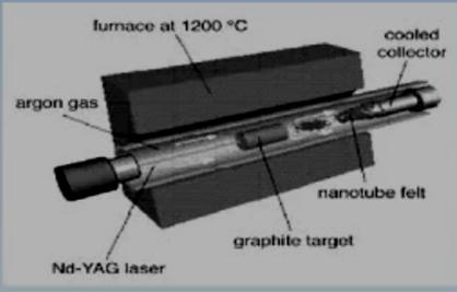
This process was developed by Dr. Richard
Smalley and co-workers at Rice
University
In
1996 CNTs
were first synthesized using a dual-pulsed laser and achieved yields of
>70wt% purity. Samples were prepared by laser vaporization of graphite rods
with a 50:50 catalyst mixture of Cobalt and Nickel at 1200°C in flowing argon,
followed by heat treatment in a vacuum at 1000°C to remove the C60 and other
fullerenes. The initial laser vaporization pulse was followed by a second
pulse, to vaporize the target more uniformly. The use of two successive laser
pulses minimizes the amount of carbon deposited as soot. The second laser pulse
breaks up the larger particles ablated by the first one, and feeds them into
the growing nanotube structure. The material produced by this method appears as
a mat of "ropes", 10-20nm in diameter and up to 100µm or more in
length. Each rope is found to consist primarily of a bundle of single walled
nanotubes, aligned along a common axis. By varying the growth temperature, the
catalyst composition, and other process parameters, the average nanotube
diameter and size distribution can be varied. The laser ablation method yields
around 70% and produces primarily single-walled carbon nanotubes with a
controllable diameter determined by the reaction temperature.
However, it is more expensive than either arc discharge or chemical vapor
deposition. Arc-discharge and laser vaporization are currently the
principal methods for obtaining small quantities of high quality CNTs.
However, both methods suffer from drawbacks. The first is that both methods
involve evaporating the carbon source, so it has been unclear how to scale up
production to the industrial level using these approaches. The second issue
relates to the fact that vaporization methods grow CNTs
in highly tangled forms, mixed with unwanted forms of carbon and/or metal
species. The CNTs thus produced are difficult to purify, manipulate, and
assemble for building nanotube-device architectures for practical applications.
Chemical Vapour Deposition:
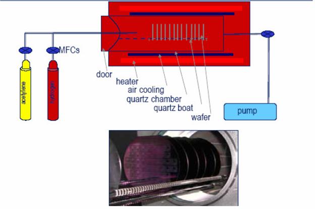
During CVD, a substrate is prepared with a layer
of metal catalyst particles, most commonly nickel, cobalt, iron, or a combination.
The metal nanoparticles can also be produced by other ways, including reduction
of oxides or oxides solid solutions. The diameters of the nanotubes that are to
be grown are related to the size of the metal particles. This can be controlled
by patterned (or masked) deposition of the metal, annealing, or by plasma
etching of a metal layer. The substrate is heated to approximately 700°C. To
initiate the growth of nanotubes, two gases are bled into the reactor: a
process gas (such as ammonia, nitrogen or hydrogen) and a carbon-containing gas (such as acetylene,
ethylene,
ethanol
or methane).
Nanotubes grow at the sites of the metal catalyst; the carbon-containing gas is
broken apart at the surface of the catalyst particle, and the carbon is
transported to the edges of the particle, where it forms the nanotubes. This
mechanism is still being studied. The catalyst particles can stay at the tips
of the growing nanotube during the growth process, or remain at the nanotube
base, depending on the adhesion between the catalyst particle and the
substrate.
If a plasma
is generated by the application of a strong electric field during the growth
process (plasma enhanced chemical vapor deposition*), then the nanotube growth
will follow the direction of the electric field. By adjusting the geometry of
the reactor it is possible to synthesize vertically aligned carbon nanotubes
(i.e., perpendicular to the substrate), a morphology that has been of interest
to researchers interested in the electron emission from nanotubes. Without the
plasma, the resulting nanotubes are often randomly oriented. Under certain
reaction conditions, even in the absence of plasma, closely spaced nanotubes
will maintain a vertical growth direction resulting in a dense array of tubes
resembling a carpet or forest.
Advantages of Multi-walled Nanotube:
The special place of double-walled carbon
nanotubes (DWNT) must be emphasized here because their morphology and
properties are similar to SWNT but their resistance to chemicals is
significantly improved. This is especially important when functionalization is required (this means
grafting of chemical functions at the surface of the nanotubes) to add new
properties to the CNT. In the case of SWNT, covalent functionalization will
break some C=C double bonds, leaving "holes" in the
structure on the nanotube and thus modifying both its mechanical and electrical
properties. In the case of DWNT, only the outer wall is modified. While
multi-wall carbon nanotubes do not need a catalyst for growth, single-wall
nanotubes can only be grown with a catalyst.
Their larger diameter favours low-ohmic contacts, they do not contain magnetic
impurities, they have very well ordered structure, high conductivity
and their mesoscopic size enables the observation of quantum interference
effects like the Aharonov-Bohm effect. The latter magnetotransport measurements
can all very well be understood.
Advantages of Single-walled Nanotube:
The results from multi-wall nanotubes are complicated
by simultaneous contributions fromconcentric nanotubes with different diameters
and chiralities. In addition, defects in the multiwalled nanotubes can lead to
electron scattering and electrical contact cannot be made reliably to all of
the constituent nanotubes. The conduction properties of the electrical contacts
can also influence electron transport. Further experimental studies of these
intriguing transport phenomena should be made on smaller diameter multi-wall
nanotubes and at low temperatures, where one-dimensional quantum effects can be
observed. The situation in multi-wall CNTs is complicated as their properties
are determined by contribution of all individual shells; those shells have
different structures, and, because of the synthesis, are usually more defective
than SWCNTs.
Applications
Field
Emission:
Buckytubes are the best known
field emitters. This is understandable, given their high electrical
conductivity, and the unbeatable sharpness of their tip (the sharper the tip, the
more concentrated will be an electric field, leading to field emission; this is
the same reason lightening rods are sharp). The sharpness of the tip also means
that they emit at especially low voltage, an important fact for building
electrical devices that utilize this feature. Buckytubes can carry an
astonishingly high current density, possibly as high as 1013 A/cm2. Furthermore, the current is
extremely stable. An immediate application of this
behaviour receiving considerable interest is in field-emission flat-panel
displays. Instead of a single electron gun, as in a traditional cathode ray
tube display, here there is a separate electron gun (or many) for each pixel in
the display. The high current density, low turn-on and operating voltage, and
steady, long-lived behaviour make buckytubes attract field emitters to enable
this application.
Molecular
Electronics:
The idea of building electronic circuits out of the essential building
blocks of materials - molecules - has seen a revival the past five years, and
is a key component of nanotechnology. In any electronic circuit, but
particularly as dimensions shrink to the nanoscale, the interconnections
between switches and other active devices become increasingly important.
Their geometry, electrical conductivity, and ability to be precisely
derived, make buckytubes the ideal candidates for the connections in molecular
electronics. In addition, they have been demonstrated as switches themselves.
Conductive
Plastics:
Much of the history of plastics over the last half century has been as a
replacement for metal. For structural applications, plastics have made
tremendous headway, but not where electrical conductivity is required, a
plastic being famously good electrical insulators.This deficiency is overcome
by loading plastics up with conductive fillers, such as carbon black and
graphite fibres (the larger ones used to make golf clubs and tennis racquets).
The loading required to provide the necessary conductivity is typically high,
however, resulting in heavy parts, and more importantly, plastic parts whose
structural properties are highly degraded.It is well established that the
higher aspect ratio of filler, the lower loading required to achieve a given
level of conductivity. Buckytubes are ideal in this sense, since they have the
highest aspect ratio of any carbon fibre. In addition, their natural tendency
to form ropes provides inherently very long conductive pathways even at
ultra-low loadings.
Applications that exploit this behaviour of buckytubes include EMI/RFI
shielding composites and coatings for enclosures, gaskets, and other uses;
electrostatic dissipation (ESD), and antistatic materials and (even
transparent!) coatings; and radar-absorbing materials.
Energy
Storage:
Buckytubes have the intrinsic characteristics desired in material used
as electrodes in batteries and capacitors, two technologies of rapidly
increasing importance. Buckytubes have a tremendously high surface area (~1000
m2/g), good electrical conductivity, and very importantly, their
linear geometry makes their surface highly accessible to the electrolyte.
Research has shown that buckytubes have the highest reversible capacity
of any carbon material for use in lithium-ion batteries. In addition,
buckytubes are outstanding materials for supercapacitor electrodes and are now
being marketed.
Catalyst
Supports
Buckytubes have an intrinsically high surface area; in fact, every atom
is not just on a surface - each atom is on two surfaces, the inside and
outside! Combined with the ability to attach essentially any chemical species
to their sidewalls provides an opportunity for unique catalyst supports. Their
electrical conductivity may also be exploited in the search for new catalysts
and catalytic behaviour.
Biomedical
Applications:
The ability to chemically modify the sidewalls of buckytubes also leads
to biomedical applications such as vascular stents, and neuron growth and
regeneration.
Fibres
and Fabrics:
Fibres spun of pure buckytubes have recently been demonstrated and are
undergoing rapid development, along with buckytube composite fibres. Such super
strong fibres will have applications including body and vehicle armour,
transmission line cables, woven fabrics and textiles.